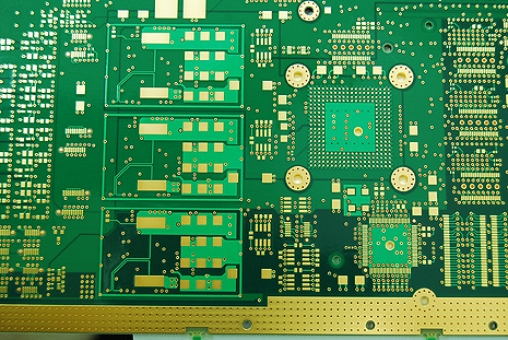
PCB Prototype
Impact of Quality of PCBs on Assembly and Product Life Cycle
Irrespective of whether the electronic product is a next generation computer system or a simple mobile handset, inside it there is a printed circuit board (PCB). Engineers design PCBs to support and connect electronic components and other hardware inside the product. The PCB usually has conductive pathways holding the electronic components together by soldering, a process for attaching different metals such as tin, silver, gold, and copper together. The process also serves to interconnect all hardware within the product.
Printed Circuit Boards (PCBs) must meet three basic requirements to be acceptable for assembly, and to establish products with longevity. According to Clyde Coombs, the author of “The Printed Circuits Handbook,” these three basic requirements are:
- The physical form of the PCB should match its intended design. Dimensions and placement of interconnection points and the coating on these interconnection points must allow proper component assembly
- The PCB must provide proper interconnection between components
- The circuit board must provide adequate insulation between interconnection points that are not to be connected
The above three items must be acceptable and remain of high quality all through the expected life of the product. As there can be several details related to the three requirements, defining the requirement for acceptability and quality for the PCB suppliers is essential to ensure they meet the three requirements. Properly implemented, the quality and acceptance criteria provide all parties a clear picture of the expectations.
Industrial Standards for PCBs
Conforming to industrial standards has the advantage of establishing a common foundation—creating level playing fields—to allow all participants to adhere to as a minimum. Adhering to industrial standards leads to avoiding many chances of failure. Everyone can easily develop knowledge about a common specification rather than interpreting endless numbers of individual company specifications. However, companies may be forced to move beyond the standards for various reasons, as their designs need to advance further than the scope defined by the standards.
Users evaluate PCB quality based on their use in products falling into three categories, called classes. These are:
Class 1: General Electronic Products, such as consumer electronic product
Class 2: Dedicated Service Products, such as those providing uninterrupted service
Class 3: High Reliability Products, such as those providing continuous service
Typically, manufacturers determine the class appropriate for their product. For instance, if a toy manufacturer wants PCBs that meet class 3 requirements, they must be willing to pay for the extra level of reliability.
Internationally, the IPC-6011 standard defines the generic performance specifications for PCBs. According to IPC-6011, the supplier of the PCB is responsible for verification of compatibility with the specifications, master drawings and patterns, and the specific manufacturing facilities and processes. In short, the supplier must ensure the PCB meets the requirements of the procurement documentation.
By default, the IPC-6011 standard applies to all circuit board types. However, this needs to be supplemented by performance specifications containing the requirements of the chosen technology such as:
IPC-6012: for Rigid PCBs
IPC-6013: for Flexible (Flex) PCBs
IPC-6014: for PCMCIA PCBs
IPC-6015: for MCM-L PCBs
IPC-6016: for HDI PCBs
IPC-6017: for Microwave PCBs
Although IPC-6012 is the most common specification used in documentation packages, manufacturers can specify the requirements according to the PCBs their electronic products use.
Acceptability of PCBs
Sometimes, it may be impossible to establish criteria for non-conformance from descriptions alone, such as from IPC-6012 and others. To circumvent this, the standard IPC-A-600 has been developed, which contains illustrations and photographs, and offers three levels of quality for each specific characteristic: Target, Acceptable, and Non-Conforming Conditions. Furthermore, the characteristics are divided into two general groups:
Externally Observable Conditions: these are features or imperfections visible on the exterior surface of the board and it is possible to evaluate them.
Fig. 2 is the image of a copper plating acceptable for a product of class 2. The acceptance criteria for the plating are:
- Not more than one void in any hole
- Not more than 5% of the holes have voids
- Any void is not greater than 5% of the length of the hole
- The void is less than 90 of the circumference of the hole
Internally Observable Conditions: these features or imperfections can only be detected, examined, and evaluated after a micro sectioning of the PCB.
The thickness of copper and insulation layers must match those specified in the design documents. Overall thickness of the board is also an important criterion.
Typically, such micro-sections are performed on coupons with the same characteristics as possessed by the actual board design. This avoids destroying a good board while testing.
General Defects in PCBs and Their Effect on Assembly
Board Warpage: If the board is not perfectly flat, it can cause several problems in the assembly process. This could be a local change in the PCB thickness or an issue of coplanarity of the PCB. It can result in potential opens from tilted components known as the teeter-totter effect, or from dropped solder connection, such as with a BGA joint. A solder joint may also potentially lose reliability from stretching. In general, leadless devices are more susceptible to PCB warpage.
With a warped board, there may also be an issue with controlling the volume of paste deposition, both for solder paste and adhesive. Warpage usually results in the stencil being unable to sit flat all over on the PCB surface, leaving gaps in between the stencil and board in certain areas. While this may result in uneven printing of solder paste across the board, there may be insufficient adhesive dispensing or adhesive may be skipped altogether in those areas.
While printing, gaps between the stencil and board may fill up with solder paste. This may cause a smear, wet bridge, or excess deposit of solder paste. Sometimes, paste fringing on the stencil after printing may cause unnecessary smears on the next print.
Uneven deposition of solder paste may result in insufficient volume being present, showing up as solder covering the pad, but with metallization showing through. As there is insufficient paste to touch the component leads, it results in unsoldered leads after reflow. For small packages, which usually decrease the total tolerance of PCB and assembly process, this may also lead to paste misalignment, resulting in cocking or tombstoning of passive chip components, impacting process yields.
During waves soldering, if via holes are unfilled and the board has warpages, the assembly can potentially lift off the wave, resulting in areas remaining unsoldered.
Solder Mask Issues: Improperly applied solder mask may cause reliability issues during assembly. One of the major issues is the missing solder mask dam between two neighboring solder pads, leading to a potential solder short or bridging during a wave soldering operation.
Normally, the solder mask is required to cover a pad all around. If there is a shift or misregistration, the solder mask may not cover the land fully, and form a pocket next to the land, exposing the neighboring pad or track. This area can subsequently fill with solder paste and create a whisker or bridge shorting the pads with the neighboring pad or track.
Another reliability issue arising from improperly applied solder mask is a smear on the pad itself causing solderability issues. This prevents solder from wetting the smeared land properly during reflow or wave soldering, leaving the pad non-solderable.
If the solder mask remains under-cured, it can lead to product reliability issues, as areas of under-cured solder mask can trap processing residues and contribute to electrical leakages or to electromechanical migration failures. Improperly cured solder resist may also allow solder to accumulate in the form of balls during wave soldering, leading to potential electrical shorts.
Issues with HAL Boards: Non-coplanar or uneven solder surfaces are a major issue for HAL finish boards. A very thin coating of HAL may lead to migration after the first reflow operation, exposing copper and leading to poor solderability in subsequent reflows.
As stencil openings normally do not match the pad perfectly, some parts of the stencil may rest on the excess solder deposit, leaving the other area of the stencil lifted away from the board. This allows solder paste to squeeze into the gap between the stencil and the board, creating issues similar to those on boards with a warpage.
Non-coplanarity of HAL boards may also lead to bumps of solder being left on pads causing the stencil to lift up and solder paste filling the underneath gap. During reflow, the excess solder may cause adjacent lands to bridge or whiskers to form between adjacent fine-pitch components. The flux in the solder paste may not be adequate for the total amount of solder from the paste and that left on the pad by the HAL process, and this may result in a grainy or disturbed joint.
Conclusion
The PCB being an electromechanical item in a product has many opportunities for failure. PCB quality is a huge subject with numerous possibilities for imperfections affecting assembly and the product life cycle. Starting from warping of the PCB surface to via failure to under-etching of traces, each aspect of PCB quality can bring the product to an abrupt halt much before its intended life cycle is over.
Top 10 High Quality Power Stencils in India, PCB Manufacturing Services, Turnkey PCB Manufacturer in India, PCB Prototype Manufacturer, PCB Fabrication and Assembly, PCB Cost Calculator, Buy Electronic Components Online, High Frequency Power Stencils in India, PCB Fabrication Services in India, Printed Circuit Board in India, Fabrication PCB, PCB Board, PCB Production, PCB Order, PCB Prototype, PCB Manufacturer, PCB Prototype Manufacturer, PCB Prototype Assembly, PCB Low Cost, PCB Prototype Fabrication, PCB Manufacturing, PCB Prototype Low Cost, Prototype PCB Board Manufacturer, PCB Manufacturing Service, Prototype Circuit Board Manufacturers, Cest PCB Prototype Service, PCB Manufacturing in India, PCB Fabrication Process, PCB Board Material, How to use Printed Circuit Board, How to use PCB Fabrication, PCB Online calculator, PCB Electronic Circuit Board, PCB Assembly Process, PCB Online Store, PCB Component Sourcing Material, PCB Power, PCB Power Login, PCB Manufacturing, PCB Fabrication, PCB Online, Online PCB design, PCB Power supply, PCB electronics, PCB design India, PCB Board price in India, PCB Service, PCB Maker, PCB Stencil, Power Circuit Board, PCB Printing Service, Custom PCB, PCB India, PCB Manufacturing Cost, PCB Order, PCB Online Quote, Buy PCB