PCB Order
How Can A Better PCB Layout Help Make Better and Faster PCB?
Commercial applications utilize high frequency bands ranging from 3 MHz to over 30 GHz. These include televisions, FM radios, radio astronomy, mobile phones, Wi-Fi and many more. Various products in the above applications make use of high frequency printed circuit boards (PCBs). The low production cost of PCBs makes them attractive to modern electronics device manufacturers. However, in smaller quantities, the price per board may be much higher.
For better and faster PCBs, designers need to pay attention to three main areas when designing the boards—construction materials, component interconnections, and layout of traces.
Construction Materials
In the design process of PCBs, designers mainly consider two major characteristics of the PCB material. One of them is the dielectric constant, and the other, the loss tangent. The dielectric constant affects the speed at which signals travel through the board. The loss tangent refers to the amount of signal lost by absorption within the material. While FR4 is a common material for constructing low-frequency circuits, for those using frequencies over 1 GHz, more premium materials are necessary.
Component Interaction
It is very important for designers of high-frequency boards to consider points of connection between components and the PCB. For instance, placement of a pad over a ground plane may act as a capacitor. Use of surface mount devices (SMD) solves the problem largely, as they have small constructional features and lead length. However, passive components, including those in SMD form, may feature non-ideal characteristics as the frequency increases. Designers must consider this and compensate for these characteristics.
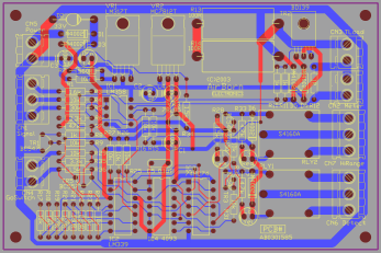
Layout of Traces
Once the designer has satisfactorily concluded the choice of construction material and the components, he/she must target achieving high-speed operations in a low-power environment. This involves:
- Minimizing on-board noise generation
- Minimizing cross-talk between traces
- Reducing any ground bounce effects
- Impedance matching
- Proper signal line termination
Minimizing On-Board Noise Generation
There are two major aspects to reducing the amount of noise generated on-board. One of them is the distribution of power throughout the board, and the other involves power noise filtering.
For distributing power throughout the PCB, designers may use either power planes or a power bus network. Typically, power planes on a multi-layer PCB consist of two or more metal layers carrying Vcc and GND to the devices. The DC resistance of such planes is low as a power plane covers nearly the full area of the PCB. Therefore, the power plane keeps the Vcc level constant while distributing it equally to all devices. It also provides noise protection, very high current-sink capability, and good shielding for the signals the PCB carries.
An alternative to the power planes is the power bus consisting or two or more wide metal traces carrying the Vcc and GND to devices. As this method is less expensive than power planes are, two-layer PCBs often use them. When designing with power bus networks, designers need to ensure the trace widths are as wide as possible. However, the power bus networks have a significantly lower DC resistance as compared to that of the power planes.
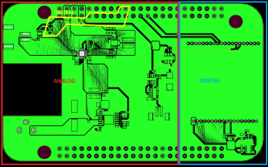
Separating planes and power buses carrying analog and digital power helps in minimizing on-board noise generation, as this prevents interaction between the two. However, all-digital systems may not have a separate analog power plane, and it may become prohibitively expensive to add a new one, unless the designer creates partitioned islands or split planes on the existing layers.
While it is advisable to separate the planes between the analog and digital power supplies on a system, some unwanted interactions may still exist between the two circuit types. Following suggestions may help to reduce the noise generation:
- Distribute power equally by using separate power planes for the analog power supply. Do not use traces or multiple signal layers to route the power supply.
- Using a ground plane adjacent to the power supply plane often helps to reduce power-generated noise.
- Place analog components only over analog ground planes and digital components only over digital ground planes.
- Isolate analog power supply lines from the digital power supply lines by using ferrite beads.
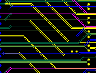
Minimizing Cross-Talk between Traces
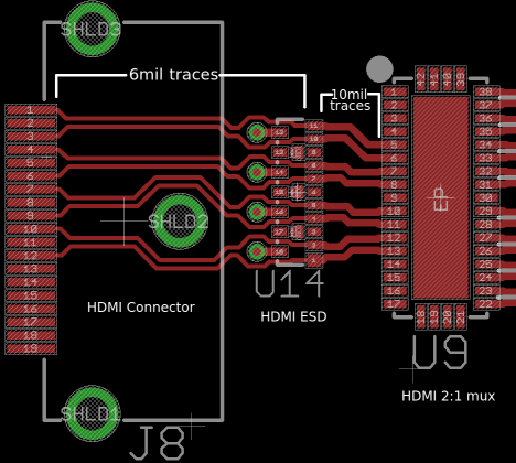
Unwanted coupling of signals between parallel traces causes crosstalk. Designers minimize crosstalk through proper routing, and using microstrip and stripline layouts in the layer stack-up.
When forced to use two signal layers next to each other, designers minimize crosstalk by routing all traces in one layer angularly to those in the next layer. Other techniques they adopt for minimizing crosstalk are minimizing the distance between the signal layer and its adjacent plane, and increasing the distance between the two signal layers.
Following suggestions may help designers in reducing crosstalk in either stripline or microstrip layouts:
- Keep maximum space between signal lines—as much as routing restrictions allow. A general rule of thumb is to space signal lines at least three times the dielectric height, or four times the trace width.
- Keep the conductor of the transmission line as close as possible to its ground plane to couple it tightly to the ground plane, and decoupling it from adjacent signals.
- Critical nets may benefit by using differential routing techniques. This may require matching the length and gyrations for each trace.
- For substantial coupling, it may help to route individual signals perpendicular to each other on different layers.
- For single-ended signals, minimizing the parallel run lengths helps to reduce crosstalk. Use short parallel sections for routing, and avoid long, coupled sections between traces.
- If it is impossible to change the separation between two traces, lowering the distance between the trace and ground plane to under 10 mils can help reduce crosstalk.
Reducing Ground Bounce Effects
With faster digital devices and decreasing output switching times, device outputs exhibit higher transient currents as they discharge load capacitances. Additionally, there may be multiple outputs of a device switching at the same time from say, logic high to a logic low. This simultaneous dumping of current into the ground can raise the potential of the ground for a moment, causing references to change, and the phenomenon is ground bounce. Predominant conditions affecting ground bounce include load capacitances, socket inductances, and the number of simultaneously switching outputs.
Designers reduce ground bounce by following design methods such as:
- Placing the via adjacent to the capacitor pad, or using short, wide traces between them
- Using wide and short traces from power pins to the power plane, island, or a decoupling capacitor. This reduces the possibility of ground bounce by lowering the series inductance, and the transient voltage drops from the power pin to the power plane.
- Individually connecting each ground pin or via to the ground plane. Daisy chaining causes sharing the ground path, increasing the return current loop resistance and inductance
- Adding decoupling capacitors as suggested by the IC manufacturer. The decoupling capacitor must be as close to the power and ground pins of the device as possible.
- Moving switching outputs as close to a package ground pin as possible
- Avoiding pull-up resistors and using more pull-down resistors
- Using multilayer PCBs with separate Vcc and GND planes, thereby utilizing the intrinsic capacitance of the Vcc-GND plane
- Using synchronous designs, as these are not affected by simultaneous switching pins
- Placing ground and power pins very close to each other, reducing the mutual inductance as the current flow is in opposite directions in the two pins.
- Minimizing the inductance in decoupling capacitors by using a bigger via size for the capacitor pads
- Minimizing lead inductance by using surface mount capacitors
- Using capacitors with lower effective series resistance
Impedance Matching and Proper Signal Line Termination
Signals reflecting back and forth along mismatched impedance lines cause ringing at the load receiver. Ringing causes false triggering of the receiver as it reduces the dynamic range of the receiver. Designers eliminate reflections by making the source impedance equal to the trace impedance as well as to the impedance of the load by using proper termination of the signal line.
For impedance matching and terminating the signal lines properly, designers take care of signal integrity by:
- Not using vias in clock transmission lines, as vias cause impedance changes and create reflections
- Keeping traces straight. Rather than using right-angled bends, use arc-shaped traces
- Using point-to-point clock traces as far as possible, and terminating clock signals to minimize reflection
- Using external devices to buffer loads and limit load capacitances
- Adding 10 to 27 ohms resistors in series with each switching output for limiting the current flow
- Placing proper terminating resistor and ensuring impedance matching between transmission line and termination is equal to the line impedance
- Sandwiching the layer routing the clock trace within reference planes to minimize noise
- Keeping trace lengths below 5 cm, impedance below 65 ohms, and maintaining the metal delay below 940 ps, inductance value lower than 40 nH, trace capacitance below 20 pF, and overall capacitance below 30 pF, especially for critical high speed routing.
Conclusion
Apart from selecting the suitable high frequency material, there is a lot a designer can do with a better PCB layout for making it work as intended at high frequencies. As each PCB is unique, it has to be custom designed for its application. Using a PCB CAD or design suite software helps the designer as the software package offers a wide range of features.
Top 10 High Quality Power Stencils in India, PCB Manufacturing Services, Turnkey PCB Manufacturer in India, PCB Prototype Manufacturer, PCB Fabrication and Assembly, PCB Cost Calculator, Buy Electronic Components Online, High Frequency Power Stencils in India, PCB Fabrication Services in India, Printed Circuit Board in India, Fabrication PCB, PCB Board, PCB Production, PCB Order, PCB Prototype, PCB Manufacturer, PCB Prototype Manufacturer, PCB Prototype Assembly, PCB Low Cost, PCB Prototype Fabrication, PCB Manufacturing, PCB Prototype Low Cost, Prototype PCB Board Manufacturer, PCB Manufacturing Service, Prototype Circuit Board Manufacturers, Cest PCB Prototype Service, PCB Manufacturing in India, PCB Fabrication Process, PCB Board Material, How to use Printed Circuit Board, How to use PCB Fabrication, PCB Online calculator, PCB Electronic Circuit Board, PCB Assembly Process, PCB Online Store, PCB Component Sourcing Material, PCB Power, PCB Power Login, PCB Manufacturing, PCB Fabrication, PCB Online, Online PCB design, PCB Power supply, PCB electronics, PCB design India, PCB Board price in India, PCB Service, PCB Maker, PCB Stencil, Power Circuit Board, PCB Printing Service, Custom PCB, PCB India, PCB Manufacturing Cost, PCB Order, PCB Online Quote, Buy PCB