PCB Fabrication and Assembly
What are Fiducial Marks and where do you use them?
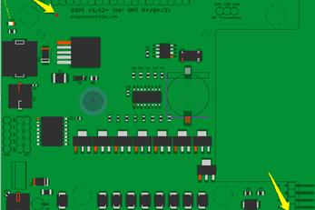
Printed Circuit Boards (PCBs) designed for assembly using automated stencil printing, pick-and-place machinery, and AOI machines, need some reference points to orient the circuit pattern to the equipment. For instance, for placing a tiny resistor of size 0201 or a chip scale micro BGA of size 2 mm x 2 mm accurately, the automated machine requires incredible precision. This machines needs to know exactly where the board is, and designers place fiducial marks on the board for just this purpose.
Therefore, fiducial marks are for the surface mount assembly machines to ensure the copper pattern on the board is oriented in the proper direction and aligned as close to perfect as possible. Most assembly machines use cameras for locating fiducial marks on the board and adjusting the component placement relative to their exact position. As board orientation is a two-axis affair, the process requires at least two fiducial marks in a non-reversible pattern. To make the arrangement non-ambiguous to the machine, IPC standards recommend three fiducial marks, although many designers often use two non-reversible marks.
Structure of a Fiducial Mark
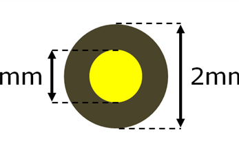
Optimally, each fiducial mark is a filled circle of solid copper. The IPC recommends a minimum diameter of 1 mm and a maximum diameter of 3 mm, with fiducial marks on the same board not varying in size by more than 25 microns. The fiducial mark should have a clear mask-free area surrounding it devoid of any other markings or any circuit feature. At the minimum, the clear area should be of size equal to the radius of the mark. However, assemblers prefer a clearance around the mark equal to the mark diameter.
Fiducial Mark requirements
While constructing a fiducial mark, it is important the designer maintains its positional accuracy, contrast, flatness, and edge clearance. For achieving high positional accuracy, the designer typically creates fiducial marks in the copper layers that will hold SMT components. This helps in registration as the fabricator etches the copper pattern in a single operation, and therefore, the positional accuracy of any surface mount pad relative to the copper fiducial will always remain the same. In contrast, drill holes and silk screen patterns cannot be used as fiducial marks, as they are added in separate operations, which means the registration is likely to vary from board to board.
Machine cameras work best with high contrast. Therefore, the fiducial mark must be of bare copper, as solder mask or silk screen on top of the copper pad will lower the contrast, and the camera may not be able to see it. Therefore, the designer and fabricator must make sure nothing obscures the copper pad of the fiducial mark. For best results, fabricators protect the bare copper mark with a nickel or tin plating, clear anti-oxidation coating, or a solder coating (HASL).
For best results, the flatness of the surface of the fiducial mark should be lower than 15 microns. Location of the fiducial mark should be no closer to the PCB edge than the sum of the fiducial clearance and 7.62 mm.
For boards in the form of panels, designers often place fiducial marks on the panel rails. However, individual boards may also have their own fiducial marks, as this helps assembly both in the panel form or as individual boards.
How machines use Fiducial Marks?
Fiducial marks help the machine to recognize the orientation and positioning of the circuit pattern on the board. Most boards use three fiducial marks, as each of them serve a purpose. Usual places for the fiducial marks are in the lower left hand corner, the lower right hand corner, and the upper right hand corner.
The first fiducial allows the machine to recognize the presence of the PCB and give it a locating X and Y coordinate or a datum point.
The second fiducial allows the machine to recognize the orientation of the circuit pattern on the board, and whether the pattern is skewed while placing the board in its clamps. Most machines can calculate the rotation of the circuit pattern down to one-tenth of a degree and compensate the component placements accordingly.
The third fiducial allows the machine to calculate any shrink of stretch the board, and hence the circuit pattern, has suffered. This is specifically helpful for large boards, as variations of very small amounts over a long distance can build up to a large value, totally ruining the accuracy of component placements at the far end of the board. The presence of the third fiducial is particularly helpful to double-sided SMT assemblies, as reflowing one side of the PCB in the oven does stretch, shrink, bow, or flex the PCB to some extent, requiring compensation when mounting components on the second side.
Conclusion
There is no hard and fast rule as to the number of fiducial marks a designer can place on the board, as long as the automated machinery can use them in a unique way. As most automated machines use fiducial marks for orientation and registration, their presence in the PCB is a necessary step during design and a checkpoint for DFM reviews.
Top 10 High Quality Power Stencils in India, PCB Manufacturing Services, Turnkey PCB Manufacturer in India, PCB Prototype Manufacturer, PCB Fabrication and Assembly, PCB Cost Calculator, Buy Electronic Components Online, High Frequency Power Stencils in India, PCB Fabrication Services in India, Printed Circuit Board in India, Fabrication PCB, PCB Board, PCB Production, PCB Order, PCB Prototype, PCB Manufacturer, PCB Prototype Manufacturer, PCB Prototype Assembly, PCB Low Cost, PCB Prototype Fabrication, PCB Manufacturing, PCB Prototype Low Cost, Prototype PCB Board Manufacturer, PCB Manufacturing Service, Prototype Circuit Board Manufacturers, Cest PCB Prototype Service, PCB Manufacturing in India, PCB Fabrication Process, PCB Board Material, How to use Printed Circuit Board, How to use PCB Fabrication, PCB Online calculator, PCB Electronic Circuit Board, PCB Assembly Process, PCB Online Store, PCB Component Sourcing Material, PCB Power, PCB Power Login, PCB Manufacturing, PCB Fabrication, PCB Online, Online PCB design, PCB Power supply, PCB electronics, PCB design India, PCB Board price in India, PCB Service, PCB Maker, PCB Stencil, Power Circuit Board, PCB Printing Service, Custom PCB, PCB India, PCB Manufacturing Cost, PCB Order, PCB Online Quote, Buy PCB