Fabrication PCB
Testing Solder Joints after Assembly
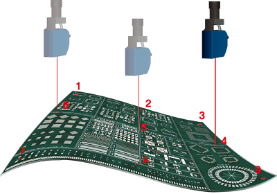
A warped printed circuit board (PCB) is one that does not sit true on a flat desktop. Although there are several reasons as to why this should happen, there are two specific causes that cause board warping. One of them is layout related, while the other is process related. If the PCB is found to be warped before the start of assembly, the problem has occurred between layout and fabrication. If the PCB was flat before, but was found warped after assembly, then the problem is likely between fabrication and assembly. However, some fabrication problems will not show up until the PCB has passed through the reflow oven.
Settling on the root cause is generally an iterative process. To discuss the issue with the fabrication or assembly shop, collecting some additional information is necessary. This could be the amount of warpage per inch, size of the board, and its thickness. Along with this information, it may be necessary to consider copper pours, placement of components, and their sizes, provided the board design is in-house.
With the above information, a discussion with the design house, fabrication, or the assembly shop may serve to highlight the issue and cause of the warpage. Once the design issue is ruled out, it may be necessary to determine if it relates to fabrication or assembly, which leads to the next step of determining a solution to the problem.
Design Issues Contributing to Warping
There can be several obscure design issues contributing to PCB warping. To be able to eliminate them before moving over to fabrication or assembly, it is necessary to know the major design contributors:
- Odd shapes or large cutouts—can cause considerable warping at any stage
- Thin board—related to number and size of components can lead to warping after assembly
- Heavy components grouped together—can cause warping during assembly. The thermal mass acts like a heat sink does, leading to uneven expansion and non-even soldering on the PCB
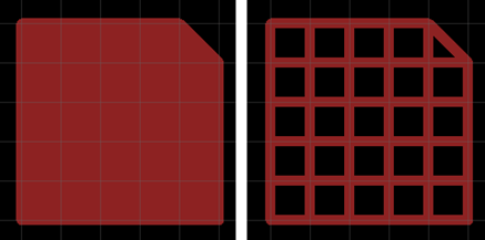
- Uneven copper pour—although copper and Polyimide/FR-4 are matched for thermal expansion, the matching is not exact. The dissimilarity is magnified for a large copper pour on one side or on a corner, leading to warping either during fabrication or during assembly. This may require the designer change over the solid copper pour to crosshatch for reducing the warpage.
Assembly Related Issues Contributing to Warping
Polyimide and FR-4 both absorb moisture from the environment. If a stack of bare boards have been stored for some time before assembly, it is customary to bake them for at least 3 hours at 80-150°C to drive out the moisture. Assembly can start once they are cooled to room temperature. Some board suppliers vacuum seal their products with a desiccant before shipping, and if the complete package is not consumed in one assembly run, it is necessary to reseal the balance along with the desiccant.
Warping in large boards may be related to the orientation as the boards enter the reflow oven. Placing the larger dimension parallel to the conveyor of the oven can prevent uneven heating between the edge of the PCB and its middle. Large boards may require additional support at the center of the PCB, and adding carriers may be necessary. Similar support may also be required for flexible PCBs during reflow.
Often small PCBs are grouped together to form panels for more efficient assembly. After assembly, operators manually separate them into individual PCBs. Manufacturers follow two methods for easing the process of separation—breakaway and v-scoring. In breakaway, most of the material between the smaller PCBs is cut away, leaving them joined by only small lands. If the panelization is large, these cutouts could lead to warping. V-scoring is an alternative method where instead of removing a part of the PCB, a v-shaped groove forms the separation line. This prevents warping of the panel during assembly, but allows the operators to separate the boards easily.
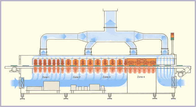
Although 3-zone reflow ovens were adequate for tin/lead soldering, with the advent of RoHS processes and lead-free soldering, reflow ovens operate at higher temperatures. Moreover, to reduce thermal shock to the PCB and components when in reflow, the temperature is gradually built up over several zones, sometimes as many as six to nine—with greater possibilities of error in the settings in one or more of the zones.
Warping may also be caused by oven loading. If the thermal profiling for a specific PCB was done for a certain number of boards in the reflow oven at the same time, the oven temperature may rise when in a subsequent run the number of boards is smaller. As the number of boards in the oven influences the thermal load, the thermal demand may not be adequate to maintain the typical reflow profile for the smaller batch of PCBs.
Clogging of airflow outlets of the reflow oven may also cause a change in the temperature-time profile for a specific PCB, resulting in uneven heating and consequently to warping. Likewise, clogging of orifice plates due to flux accumulation may also limit the forced convection flow, causing the boards to heat up unevenly.
Preventing Warping of PCBs
For PCBs meant for surface mount technology, the IPC-6012 standard defines the maximum camber and twist or warping to 0.75%, while for other types (through-hole technology) this is relaxed to 1.5%. However, most electronic assembly plants dealing with double/multilayer boards prefer to limit warping to between 0.7 and 0.75%. Rigid PCBs with thicknesses of around 1.6 mm and using SMDs and BGAs can only stand warping to the extent of 0.5%, while others using PoP can handle warpages of only 0.3% or less.
Storing PCBs properly before assembly is crucial in preventing warpage. Stacking PCBs on their edge cannot guarantee they will be vertical all the while, and the combined weight of the PCBs will ultimately cause a camber. Therefore, storing them horizontally on a flat surface is essential.
It is usual for PCBs to absorb moisture from the surroundings. Storing them in an area where the temperature and humidity is under control is the ideal solution. Where it is impractical to control the environment within the entire store, use of desiccants to control the moisture within a sealed container may also help in preventing PCBs from acquiring moisture during storage.
As PCB fabricators use heat to form multilayer boards, re-application of heat to warped bare boards should be helpful in straightening them as well. This may require heavy-pressing the boards between heated smooth steel plates for 3 to 6 hours and baking the PCBs 2 to 3 times
Top 10 High Quality Power Stencils in India, PCB Manufacturing Services, Turnkey PCB Manufacturer in India, PCB Prototype Manufacturer, PCB Fabrication and Assembly, PCB Cost Calculator, Buy Electronic Components Online, High Frequency Power Stencils in India, PCB Fabrication Services in India, Printed Circuit Board in India, Fabrication PCB, PCB Board, PCB Production, PCB Order, PCB Prototype, PCB Manufacturer, PCB Prototype Manufacturer, PCB Prototype Assembly, PCB Low Cost, PCB Prototype Fabrication, PCB Manufacturing, PCB Prototype Low Cost, Prototype PCB Board Manufacturer, PCB Manufacturing Service, Prototype Circuit Board Manufacturers, Cest PCB Prototype Service, PCB Manufacturing in India, PCB Fabrication Process, PCB Board Material, How to use Printed Circuit Board, How to use PCB Fabrication, PCB Online calculator, PCB Electronic Circuit Board, PCB Assembly Process, PCB Online Store, PCB Component Sourcing Material, PCB Power, PCB Power Login, PCB Manufacturing, PCB Fabrication, PCB Online, Online PCB design, PCB Power supply, PCB electronics, PCB design India, PCB Board price in India, PCB Service, PCB Maker, PCB Stencil, Power Circuit Board, PCB Printing Service, Custom PCB, PCB India, PCB Manufacturing Cost, PCB Order, PCB Online Quote, Buy PCB